Method for creating high-precision additive manufacturing finite element model
Technical Field
The invention belongs to the field of additive manufacturing, relates to metal additive manufacturing finite element analysis, and particularly relates to a method for creating a high-precision additive manufacturing finite element model.
Background
The additive manufacturing technology is based on the forming thought of 'discrete-accumulation', firstly two three-dimensional CAD solid models are generated in a computer, then the models are sliced and layered according to a certain thickness, namely three-dimensional structure information is converted into a series of approximate two-dimensional outlines, the obtained two-dimensional outline information of each layer is checked and corrected and converted into numerical control processing information, then under the control of a control system, high-energy beams (laser, electron beams, electric arcs and the like) melt raw materials on a base material according to a certain scanning path and fill the given two-dimensional outlines to form a cladding layer, and the process is continuously repeated and a three-dimensional solid component is formed by layer-by-layer accumulation. The additive manufacturing technology has the characteristics of no mould, rapidness, low cost, near-net forming and the like, and is widely applied to the fields of aerospace, medical treatment, automobiles, engineering and the like. However, many drawbacks still exist in additive manufacturing, wherein residual stress and deformation are two main factors limiting the development of metal additive manufacturing technology. The traditional industrial test method is used for researching the residual stress and the deformation, so that the efficiency is low, the cost is high, and the method has great limitations. Finite element analysis is an effective tool for predicting the thermal stress field of metal additive manufacturing, and therefore most scholars choose to use finite element analysis to study the residual stress and deformation of metal additive manufacturing components.
In the additive manufacturing process, especially for high-energy beam additive manufacturing of metal, in the initial stage of processing, since the substrate for the support member is at room temperature, the substrate has a strong cooling effect on the molten pool, and the width and depth of the molten pool tend to be limited to a certain extent. As the printing process progresses, the substrate is gradually heated and the cooling effect on the molten pool is reduced, so that the thickness of the deposited layer gradually increases. Thus, the temperature of the substrate directly determines the thickness of the deposited layer, and for each layer of the printing process, the last deposited layer is the substrate, so the residual temperature of the last deposited layer will determine the deposited thickness of that layer.
However, existing finite element models for predicting the additive manufacturing thermal force field all use average layer thickness, that is, all cladding layer thicknesses are kept consistent, and the values are obtained through calculation of the height of a component and the number of deposited layers. Obviously, the existing additive manufacturing finite element model cannot simulate and reproduce the actual additive manufacturing process to the maximum extent. The stress-strain field and the deformation of the additive manufacturing component have historical correlation, and the residual stress and the deformation are strongly influenced by the actual deposition process, so that the thermal-stress field evolution of the additive manufacturing component cannot be accurately predicted by adopting the existing additive manufacturing finite element model. Therefore, the existing additive manufacturing finite element model needs to be further optimized to improve the precision of the model so as to meet the requirement of accurately predicting the stress-strain field evolution of the additive manufacturing component, and the method has important significance for relieving or even eliminating the residual stress and deformation cracking of the additive manufacturing component.
Disclosure of Invention
Aiming at the problems in the prior art, the invention provides a method for creating a high-precision additive manufacturing finite element model, which can effectively reproduce experimental results by considering the change of the thickness of a deposition layer in the actual processing process and carrying out self-adaptive modeling according to the residual temperature of the previous layer and the deposition thickness of the first layer.
The invention is realized by the following technical scheme:
a method of creating a high-precision additive manufacturing finite element model, comprising the steps of,
step one, measuring a metal additive manufacturing in-situ temperature field;
under the same technological parameters, a thermal imager is utilized to carry out whole-process monitoring on temperature fields in the experimental process of metal additive manufacturing single-channel single-layer and single-channel multi-layer (more than 10 layers) to obtain the temperature field in the deposition process of each layer;
step two, calculating the initial temperature T of the substrate when the ith layer is depositedi-1;
When i is 1, the initial temperature of the substrate is room temperature;
when i is greater than 1, the initial temperature of the substrate is the residual temperature of the deposition layer of the (i-1) th layer;
processing real-time temperature field data monitored by a thermal imager, extracting the residual temperature of the layer after the i-th layer is finished, and obtaining the average residual temperature T of the i-th layeriI.e. the initial temperature of the substrate of the (i + 1) th layer;
the number of layers at which the residual temperature reached stability was recorded as critical layer n, and the average residual temperature of this layer was recorded as TnI.e. from the nth layer, flatAll residual temperatures remained unchanged and are all TnThe layer thicknesses likewise remaining constant and all being hn;
Step three, calculating the thickness h of the deposited layer of the ith layer of the componenti;
Cutting the single-channel multilayer sample along a vertical plane, and measuring the total height H of all deposited layers before the layer thickness is unchanged
nAnd measuring the thickness h of the single-pass single-layer sample cladding layer
1And a width d; a constant value of the layer thickness difference deltah between the deposited layers is obtained,
when i is<n, the thickness of the deposition layer is gradually increased in the initial deposition stage, and the thickness of the deposition layer of the i-th layer is hi=h1+(i-1)Δh;
When i is more than or equal to n, the thickness of the deposition layer is kept unchanged, and the thickness of the deposition layer of the i-th layer is
Step four, establishing the deposition thickness h of the ith layer of the componentiAnd initial temperature T of substratei-1Is in the mapping relation hi=F(Ti-1);
Step five, depositing thickness h based on the measured first layer1And width d, and the geometric dimension of the substrate, creating a finite element model of the layer 1, and calculating the thermal stress field of the layer 1 in the deposition process;
step six, calculating the layer thickness h of the ith layer modeliWherein i>1;
Calculating the average residual temperature of the i-1 th layer, namely the initial temperature T of the substrate of the i-th layeri-1Then using hi=F(Ti-1) Calculating the layer thickness h of the ith layeri;
Step seven, sequentially calculating the thermal stress field of the ith layer in the deposition process from the 2 nd layer;
based on layer i-1Finite element model and layer thickness h of ith layeriCreating a finite element model of the deposition layer of the ith layer, endowing material properties to the finite element model and dividing the finite element model into grids, applying heat and force boundary conditions to the finite element model of the ith layer by adopting process parameters consistent with those in the measurement of the in-situ temperature field, and calculating the thermal stress field in the deposition process of the ith layer;
step eight, judging whether the ith cladding layer is the last layer; and if the ith cladding layer is the last layer, finishing modeling of the finite element model, otherwise, entering the step six, and circulating until modeling calculation of the finite element models of all the deposition layers is finished.
Preferably, in the step one, the number of layers in the single-pass multilayer experiment process is greater than 10.
Preferably, the specific steps of step four are as follows,
at the initial temperature T of the substratei-1With variable X, deposit thickness h of ith layeriMaking speckle patterns of X and Y for Y variables, and using curve fitting method to create deposition thickness hiAnd initial temperature T of substratei-1Is in the mapping relation hi=F(Ti-1)。
Preferably, the concrete steps of the step five are as follows,
deposition thickness h of first layer based on measurement1And the width d and the geometric dimension of the substrate, creating a finite element model of the substrate and the 1 st deposition layer, endowing material attributes to the finite element model and dividing the finite element model into grids, applying thermal and force boundary conditions to the 1 st deposition layer thermal coupling model by adopting process parameters consistent with those in the in-situ temperature field measurement, and calculating the thermal stress field of the metal additive manufacturing component by adopting a sequential coupling mode.
Further, the sequential coupling mode means that a thermal field is calculated first, and the result of the thermal field is used as a boundary condition for calculating the stress field.
Compared with the prior art, the invention has the following beneficial technical effects:
the thickness of the deposition layer is automatically calculated through the initial temperature of the substrate (the substrate of the ith layer is the deposition layer of the (i-1) th layer), and the finite element model of the deposition layer can be automatically established according to the method, so that the thickness of each deposition layer of the corresponding additive manufacturing component model is determined, the thickness of the deposition layer of the model is kept consistent with the thickness of the deposition layer of the actual additive manufacturing component, the consistency of the simulation process and the actual processing process is ensured, and the accuracy of the model in predicting the forming process of the additive manufacturing component is effectively improved. Compared with the existing additive manufacturing finite element model, the created high-precision finite element model is not created at one time, and the model of the next layer is created based on the calculation result of the previous layer, so that the method is more suitable for the forming characteristic of dynamic self-adaption in the additive manufacturing process. The method is not only applied to additive manufacturing of a macroscopic thermal stress field finite element model, but also can be used for researching mesoscopic or microscopic models of a flow field, solute diffusion and tissues. The method has wide application range, and can be applied to the field of high-energy beam additive manufacturing and the field of welding such as surfacing.
Drawings
FIG. 1 is a flow chart of the method of the present invention.
Fig. 2 is an experimental apparatus for measuring a laser additive manufacturing in-situ temperature field according to an embodiment of the present invention.
FIG. 3 shows the initial temperature of the substrate during deposition of each layer of the single pass 20 layer member in accordance with the present invention.
Fig. 4 shows the thickness variation of each deposition layer of the single 20-layer member according to the example of the present invention.
FIG. 5 is a rectangular frame member of Ti-6Al-4V titanium alloy printed by laser additive manufacturing techniques as described in the examples of the invention.
Fig. 6a shows a finite element model of a component with an average layer thickness for an additive manufacturing finite element model according to the prior art.
Fig. 6b is an enlarged view of the structure at a in fig. 6 a.
FIG. 7a is a schematic diagram of an additive manufactured high precision finite element model according to an example of the present invention.
Fig. 7B is an enlarged view of the structure at B in fig. 7 a.
FIG. 8 is a graph of the residual temperature field of the first layer of the high-precision finite element geometric model in an example of the present invention.
FIG. 9 compares the temperature history calculated by the two models with the experimental results.
FIG. 10 compares the calculated deformation history of the two models with the experimental results.
In the figure: the device comprises a thermal imager 1, a substrate 2, deposited metal 3 and a high-energy beam 4.
Detailed Description
The present invention will now be described in further detail with reference to specific examples, which are intended to be illustrative, but not limiting, of the invention.
In the initial deposition stage of additive manufacturing, the thickness of the deposition layer is gradually increased from thin to thick due to the heat storage effect of the cold substrate, but the change of the thickness of the deposition layer in the actual processing process is ignored in the existing additive manufacturing model, the average layer thickness is adopted in the model, so that the calculation result of the model is obviously different from the experimental result, and the experimental result cannot be effectively reproduced in the simulation process.
In order to solve the problem that a finite element model for analyzing the evolution of an additive manufacturing thermal-stress field is not in accordance with the actual printing process, the invention designs a method for creating a high-precision additive manufacturing finite element model based on the fact that the thickness of a cladding layer is gradually increased in the initial stage of additive manufacturing. In the additive manufacturing process, the thickness of the next cladding layer model is calculated according to the residual temperature of the previous layer and the deposition layer thickness of the first layer, and then adaptive modeling is carried out, so that the consistency of the simulation process and the actual machining process of the additive manufacturing component is ensured, and the layer thickness is adaptive.
Step one, carrying out a metal additive manufacturing in-situ temperature field measurement experiment; under the same technological parameters, a thermal imager is utilized to carry out whole-process monitoring on the temperature field in the experimental process of metal additive manufacturing single-channel single-layer or single-channel multi-layer (more than 10 layers) to obtain the temperature field in the deposition process of each layer.
Step two, calculating the initial temperature T of the substrate when the ith layer is depositedi-1(ii) a When i is 1, the initial temperature of the substrate is room temperature, T0Is at room temperature; when i is>1, the i-1 deposition layer is the substrate of the i-th layer, so the initial temperature of the substrate is the residual temperature of the i-1 deposition layer. Processing the real-time temperature field data monitored by the thermal imager, and processing each dataAfter the deposition layer is finished, the residual temperature of the layer is extracted, and the average residual temperature T of the layer (i-th layer) is obtainediI.e. the initial temperature of the substrate of the (i + 1) th layer. Since the temperature field centered on the molten pool becomes dynamically stable as the number of deposited layers increases, the number of layers at which the residual temperature becomes stable is recorded as the critical layer n, and the average residual temperature of the layer is recorded as TnI.e. the average residual temperature, starting from the nth layer, is considered to remain unchanged and is TnThe layer thicknesses likewise remaining constant and all being hn。
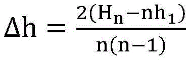
Step three, calculating the thickness h of the deposited layer of the ith layer of the component
i(ii) a Cutting the single-channel multilayer sample along a vertical plane, and measuring the total height H of all deposited layers before the layer thickness is unchanged
nIn addition, the thickness h of the single-pass single-layer sample cladding layer is measured
1And a width d. Provided that the layer thickness difference between the deposited layers is a constant quantity Δ h, there is
Thus can be solved
When i is<n, i.e. the thickness of the deposition layer gradually increases in the initial deposition stage, the thickness of the deposition layer of the i-th layer is h
i=h
1+ (i-1) Δ h. When i is more than or equal to n, namely the thickness of the deposition layer is kept unchanged, the thickness of the deposition layer of the ith layer is
Step four, establishing the deposition thickness h of the ith layer of the componentiAnd initial temperature T of substratei-1The mapping relationship of (2); at the initial temperature T of the substratei-1With variable X, deposit thickness h of ith layeriFor the Y variable, X, Y speckle patterns were made and the deposition thickness h was created using a curve fitting methodiAnd initial temperature T of substratei-1Is in the mapping relation hi=F(Ti-1)。
In the fifth step, the step of,calculating a thermal stress field in the deposition process of the layer 1; deposition thickness h of first layer based on measurement1And the width d and the geometric dimension of the substrate, creating a finite element model of the substrate and the 1 st deposition layer, endowing material attributes to the finite element model and reasonably dividing grids of the finite element model, applying thermal and force boundary conditions to the 1 st deposition layer thermal coupling model by adopting process parameters consistent with experiments, and calculating the thermal stress field of the metal additive manufacturing component by adopting a sequential coupling mode. The sequential coupling mode firstly calculates a temperature field, and the temperature field result is used as a boundary condition for calculating a stress field.
Step six, calculating the ith (i)>1) Layer thickness h of the layer modeli(ii) a Firstly, an algorithm is designed to carry out automatic processing on the temperature field result of the i-1 th layer, and the average residual temperature of the i-1 th layer, namely the initial temperature T of the substrate of the i-th layer is calculatedi-1Then using hi=F(Ti-1) Calculating the layer thickness h of the ith layeri。
Step seven, sequentially calculating the thermal stress field of the ith layer in the deposition process from the 2 nd layer; finite element model based on the i-1 th layer and the thickness h of the i-th layeriCreating a finite element model of the deposition layer of the ith layer, endowing material properties to the finite element model, reasonably dividing a grid for the finite element model, applying thermal and force boundary conditions to the finite element model of the ith layer, and calculating a thermal stress field in the deposition process of the ith layer.
Step eight, judging whether the ith cladding layer is the last layer; if the ith cladding layer is the last layer, the simulation process is ended, otherwise, the step six is carried out, and the process is circulated until the modeling calculation of all the deposition layers is completed.
The present invention will now be described in further detail with reference to the accompanying drawings. These drawings are simplified schematic views, and merely illustrate the basic structure of the present invention in a schematic manner, and therefore, only show the components related to the present invention.
In the following, an additive manufacturing rectangular component manufactured by using a laser stereolithography technique and having a substrate clamped on one side is taken as a representative, and it is described how to create an additive manufacturing high-precision finite element model in a metal additive manufacturing process, and a technical schematic diagram of the present invention is shown in fig. 1.
First, a single pass 20-layer additive manufacturing experiment is performed, as shown in fig. 2, a thermal imager 1 is used to monitor the temperature field of the
deposit metal 3 deposited on the
substrate 2 by the high-
energy beam 4 in real time during the forming process, and the temperature field during each layer of deposition is obtained. The material adopts Ti-6Al-4V titanium alloy, the laser is a fiber laser, the wavelength of the fiber laser is 960-1200nm, the laser power is 1500W, and the diameter of a light spot is 4 mm. Fig. 3 is a graph of the initial temperature of the substrate during deposition of layers calculated based on temperature field data measured by thermal imaging. In the evolution course of the thickness of the deposition layer of the single-pass 20-layer member shown in fig. 4, it can be seen that the thickness of the deposition layer is gradually increased from thin to thick at the initial stage of deposition, rather than being uniform all the time. Starting from the 7 th layer deposition, the deposited layer thickness remains substantially constant, which corresponds to the substrate initial temperature change. The layer thickness of the 1 st layer was measured to be 0.2mm and the total layer thickness of the first 7 layers was 2.45 mm. According to
The difference in layer thickness between the deposited layers was found to be 0.05mm, so the deposited layers of the 2 nd, 3 rd, 4 th, 5 th, 6 th and 7 th layers were 0.2mm, 0.25mm, 0.3mm, 0.35mm, 0.4mm, 0.45mm and 0.5mm, respectively, and the model thicknesses of the deposited layers of the 8 th and subsequent layers were all 0.5 mm. Then, the initial temperature T of the substrate when the number of layers i is less than or equal to 7 can be calculated according to the experimental measurement results
iThe relation with the number i of layers is T
i95i-65, deposition layer thickness h
iThe relation with the number i of layers is h
i0.05i +0.15, a deposition layer thickness h can be obtained
iAnd initial temperature T of substrate
i-1Of (2) a mapping relation
A 44-layer rectangular frame member was fabricated using the same process parameters as the single 20-layer experiment, as shown in fig. 5, with one end of the substrate clamped and the other end free to warp during printing. Measuring the geometric dimension of the rectangular component manufactured by the additive manufacturing, calculating the average thickness of the deposition layer through the height of the rectangular frame and the number of the deposition layers, wherein the average thickness is 0.47mm, establishing an equal-layer thickness additive manufacturing finite element model by using finite element analysis software, and calculating the thermal-force field evolution process of the rectangular component manufactured by the additive manufacturing by adopting a sequential coupling mode, wherein the thickness of each deposition layer model is 0.47mm as shown in fig. 6a and 6 b.
For the created additive manufacturing high precision finite element model proposed by the present invention, fig. 7a and 7b are schematic diagrams of the created finite element model of all deposition layers. First, a finite element model of the substrate and layer 1 deposition was created based on the first layer deposition thickness of 0.2 mm. And setting the same process parameters as those of the actual additive manufacturing process for the two additive manufacturing models, applying the same boundary conditions to the models, and calculating the thermal stress field of the layer 1 deposition process. FIG. 8 shows the residual temperature field of the layer 1 deposition, the result of the temperature field is automatically processed, and the average residual temperature of the layer 1 deposition, i.e. the initial substrate temperature t of the
layer 2 deposition
2=T
1Then use
The layer thickness h of the 2 nd layer is calculated
2. Creating a finite element model of the 2 nd layer deposition layer, endowing material properties to the finite element model, reasonably dividing grids of the finite element model, applying thermal boundary conditions, and calculating a thermal stress field in the 2 nd layer deposition process. And so on until the modeling calculations for all the sedimentary layers are completed.
To reduce the amount of computation, only the first 12 layers of deposition process of the rectangular member were calculated using an additive manufacturing finite element model of layer thickness variation. Fig. 9 is a comparison of the temperature history calculated using two additive manufacturing finite element models of uniform layer thickness and layer thickness variation with experimental results, and it was found that the temperature curves calculated by the models for the two different layer thickness settings have a small difference and are substantially negligible. Fig. 10 is a comparison of deformation history calculated by two additive manufacturing finite element models with uniform layer thickness and layer thickness variation and experimental results, and the result shows that the deformation curve calculated by the additive manufacturing finite element model with layer thickness variation has a better matching degree with the experimental results. Therefore, the method can effectively improve the precision and accuracy of the finite element model for additive manufacturing, and has important significance for accurately predicting the evolution of the additive manufacturing thermal stress field.